The design challenge
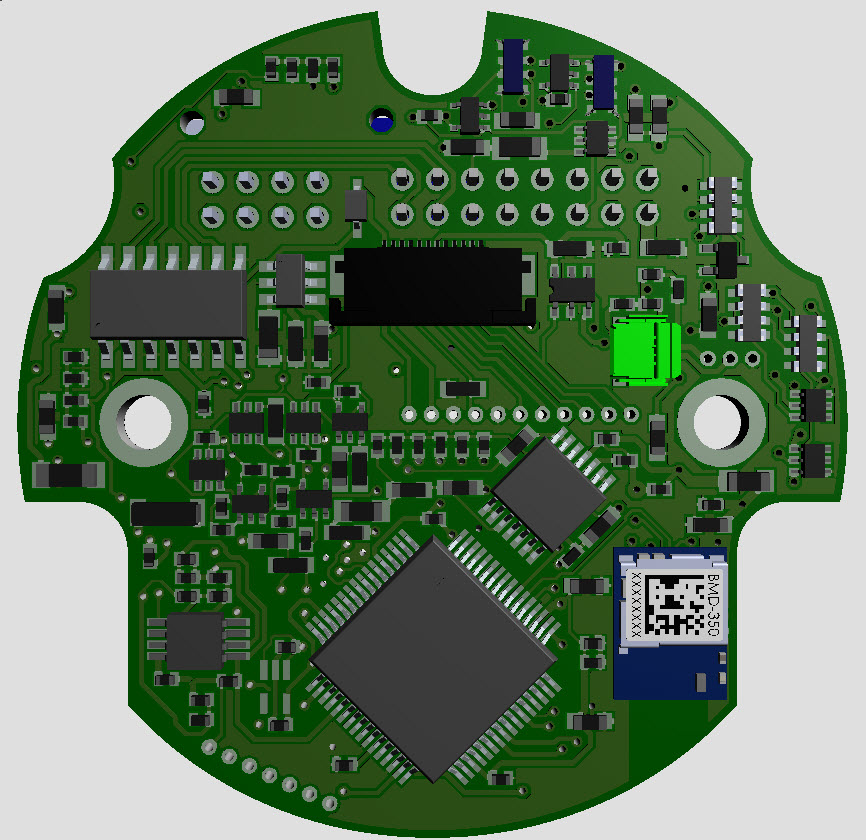
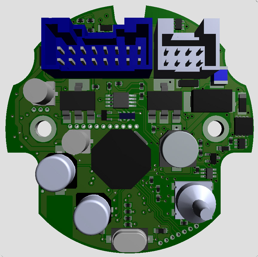
The small circular outline left limited routing area. Mechanical cutouts and mounting holes reduced usable space further, while large components and pads on the reverse side conflicted with conventional through-hole via placement.
Design approach
I used blind vias where through-hole vias would interfere with the components behind the board. Three groups of untented vias provided test access to programming pins and control signals for production testing. Two harness connectors supplied additional electrical connections.
What this demonstrates
PCB layout is not just about connecting nets. Mechanical geometry, assembly clearance, and manufacturing test access all shape the routing strategy. This project required those tradeoffs to be considered together.
Original project photos
Click any photograph to view the full-resolution original.